
* This blog post is an English translation of an article originally published in Japanese on August 18, 2025.
Introduction
Hello, this is Hirooka, an engineer.
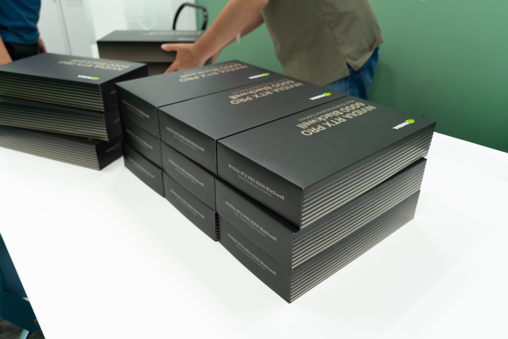
The “NVIDIA RTX PRO 6000 Blackwell Max-Q Workstation Edition” (hereafter, 6000 Blackwell Max-Q) has been released, and we were able to get our hands on a few.
Starting with this article, I will explain the performance of the 6000 Blackwell Max-Q over several installments. In this first part, I will introduce its features and performance based on NVIDIA’s datasheet, comparing it with the high-end GPU, the NVIDIA H100 PCIe (hereafter, H100 PCIe).
At the end of this article, you will find a comprehensive comparison table that includes the specs of the NVIDIA GeForce RTX 5090 and NVIDIA RTX 6000 Ada for reference, in addition to the H100 PCIe, which is our primary comparison point.
Summary
The 6000 Blackwell Max-Q is the latest workstation GPU, announced at GTC in March 2025, featuring the Blackwell architecture. The Blackwell architecture GPUs include the following series:
- GeForce RTX 50 Series
- Blackwell RTX PRO Series
- HPC-oriented series: GB200, B200, B100
This unit is a power-efficient model for workstations within the Blackwell RTX PRO series, achieving a power consumption of 300W, compared to its sibling model, the 6000 Blackwell Workstation Edition (600 W).
Next, we will examine its performance in the following order:
- Theoretical Performance
- Differences in the “Streaming Multiprocessor (SM),” the core of the GPU’s compute units
- Differences across the entire chip
- GPU Memory
- Power Efficiency
Theoretical Performance Comparison
To understand the positioning of the 6000 Blackwell Max-Q, let’s compare its theoretical performance with the H100 PCIe.
| 6000 Blackwell Max-Q | H100 PCIe | |
|---|---|---|
| Architecture | Blackwell (GB202) | Hopper (GH100) |
| FP64 Performance (TFLOPS) | 1.71 | 25.6 |
| FP32 Performance (TFLOPS) | 109.7 | 51.2 |
| INT32 Performance (TOPS) | 109.7 | 25.6 |
| TF32 Performance (TFLOPS) | 438.9 | 756 |
| INT8 Performance (TOPS) | 1755.7 | 3026 |
| FP8 Performance (FP16 Accumulate) (TFLOPS) | 1755.7 | 3026 |
| FP8 Performance (FP32 Accumulate) (TFLOPS) | 1755.7 | 3026 |
| FP4 Performance (FP32 Accumulate) (TFLOPS) | 3511.4 | N/A |
| RT Core Performance (TFLOPS) | 332.6 | N/A |
First, regarding the architecture, as mentioned at the beginning, the 6000 Blackwell Max-Q is a GPU that adopts the new “Blackwell” architecture, while the H100 PCIe uses the previous “Hopper” architecture. The Blackwell generation brought changes to the configuration of arithmetic units within the SM, the generation of the units themselves, and memory performance. We will examine these details later.
Next, in FP64 performance, the H100 PCIe is approximately 15 times more powerful than the 6000 Blackwell Max-Q. For scientific and technical computing that heavily utilizes FP64, the H100 PCIe would be the more suitable choice.
In stark contrast to FP64, the 6000 Blackwell Max-Q’s FP32 performance is double that of the H100 PCIe. This FP32 performance difference is likely due more to the difference in the number of CUDA cores, which we’ll discuss later, rather than the architectural generation gap.
For INT8/FP8/TF32 performance, primarily used for machine learning model training and inference, the H100 PCIe is about 1.7 times faster. If high performance for machine learning is required, the H100 PCIe is the better option.
FP4 performance is listed only for the 6000 Blackwell Max-Q. This is because FP4 computation was first supported at the hardware level with the Blackwell architecture. Currently, there are few machine learning models or processes that use FP4, but it is expected that scenarios requiring FP4 will increase in the future. The 6000 Blackwell Max-Q is expected to excel in such situations.
Additionally, the H100 PCIe, which lacks video output capabilities, does not have RT Cores. Therefore, RT Core performance is only listed for the 6000 Blackwell Max-Q.
To compare cost-performance, I calculated the performance per 10,000 yen by dividing each GPU’s theoretical performance by its price. The H100 PCIe is priced at 4.7 million yen (AKIBA PC Hotline! Editorial Dept. 2023b), and the 6000 Blackwell Max-Q is set at 1.6 million yen (AKIBA PC Hotline! Editorial Dept. 2023a).
| 6000 Blackwell Max-Q | H100 PCIe | |
|---|---|---|
| Architecture | Blackwell (GB202) | Hopper (GH100) |
| FP64 Performance (TFLOPS) | 0.0107 | 0.0545 |
| FP32 Performance (TFLOPS) | 0.686 | 0.109 |
| INT32 Performance (TOPS) | 0.686 | 0.0545 |
| TF32 Performance (TFLOPS) | 2.74 | 1.61 |
| INT8 Performance (TOPS) | 11.0 | 6.44 |
| FP8 Performance (FP16 Accumulate) (TFLOPS) | 11.0 | 6.44 |
| FP8 Performance (FP32 Accumulate) (TFLOPS) | 11.0 | 6.44 |
| FP4 Performance (TFLOPS) | 21.9 | N/A |
| RT Core Performance (TFLOPS) | 2.08 | N/A |
The FP64 performance of the 6000 Blackwell Max-Q is about one-fifth that of the H100 PCIe per 10,000 yen. This difference stems from the different number of FP64 arithmetic units in the two GPUs. Looking at this price-performance ratio and the hardware’s arithmetic unit count, the H100 PCIe is more cost-effective for processes that heavily use FP64 and require high precision, such as scientific and technical computing.
For FP32 performance, the 6000 Blackwell Max-Q offers 6 times the performance per 10,000 yen compared to the H100 PCIe. The 6000 Blackwell Max-Q is superior in both cost-performance and theoretical FP32 performance.
For TF32/INT8/FP8, used in machine learning model training and inference, the 6000 Blackwell Max-Q provides over 1.5 times the performance per 10,000 yen compared to the H100 PCIe. While the H100 PCIe excels in absolute performance, the 6000 Blackwell Max-Q wins in cost-performance. Therefore, if cost is a priority, the 6000 Blackwell Max-Q is suitable, whereas if maximum performance is required, the H100 PCIe is the better choice.
Hardware Comparison
From here, we will explore how the differences in theoretical performance arise from differences in hardware specifications. The points of comparison are:
- Performance of a single SM
- Changes across the entire chip
- Memory performance
- Power efficiency
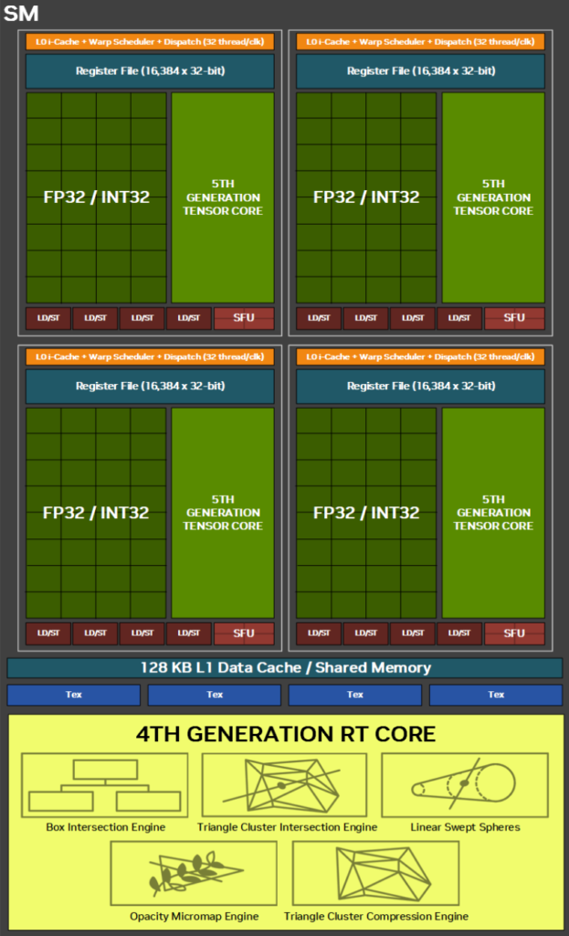
Newly Designed Streaming Multiprocessor
| 6000 Blackwell Max-Q | H100 PCIe | |
|---|---|---|
| CUDA Cores / SM | 128 | 128 |
| FP32 Cores / SM | 128 | 128 |
| FP64 Cores / SM | 2 | 64 |
| INT32 Cores / SM | 128 | 64 |
With the Blackwell architecture, the internal structure of the SM in the 6000 Blackwell Max-Q has also been redesigned.
Unification of INT32/FP32 Cores
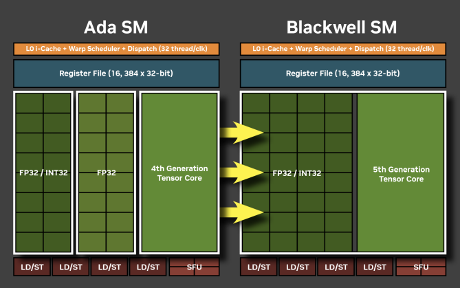
One of the major changes is in the cores that perform INT32 operations. In previous generations like Ada Lovelace and Hopper, INT32 operations were handled by a subset of cores. In contrast, with Blackwell, all cores can execute both FP32 and INT32 operations. This significantly improves the INT32 performance of the 6000 Blackwell Max-Q, which is expected to be effective not only for INT32-heavy workloads but also for workloads with a mix of INT32 and FP32 operations. However, this does not mean that a single core can execute both FP32 and INT32 operations simultaneously. Therefore, even in workloads with a complex mix of FP32/INT32, it’s likely that maximum performance can only be achieved if there are enough INT32 and FP32 instructions to keep the pipelines within each core full.
Instruction Throughput per SM
Now, let’s delve deeper into the SM’s compute performance by referencing the instruction throughput table published by NVIDIA (NVIDIA 2025a).
| Compute Capability | 6000 Blackwell Max-Q | H100 PCIe |
|---|---|---|
| FP64 Add/Multiply/FMA Instructions | 2 | 64 |
| FP32 Add/Multiply/FMA Instructions | 128 | 128 |
| INT32 Add/Subtract/Multiply/FMA | 128 | 128 |
| INT32 Compare/Min/Max Instructions | 128 | 64 |
| INT64 Add Instructions | 64 | 32 |
| warp vote | 128 | 64 |
The table above shows the instruction throughput for each GPU based on its Compute Capability (CC), referencing CUDA 13.0.0 documentation. The H100 PCIe is CC 9.0, and the 6000 Blackwell Max-Q is CC 12.0. Note that values may differ in other versions of the CUDA documentation.
As mentioned earlier, in the 6000 Blackwell Max-Q, the arithmetic units for INT32 and FP32 have been unified. The instruction throughput table confirms that FP32 and INT32 operations have the same throughput. Compared to the H100 PCIe, the 6000 Blackwell Max-Q has a higher throughput for INT32 compare/min/max instructions. While the INT32 addition throughput is the same for both GPUs, improvements at the SASS (CUDA assembly language) level mean that the 6000 Blackwell Max-Q can likely achieve higher INT32 throughput in practice (NVIDIA 2025b). Other operations like subtraction, multiplication, and fused multiply-add have also been improved in the Blackwell generation, so actual performance may differ significantly.
The FP32 instruction throughput is 128 for both the H100 PCIe and the 6000 Blackwell Max-Q. This indicates that the difference in FP32 performance between these GPUs is not due to differences within a single SM.
The 6000 Blackwell Max-Q also shows an increased instruction throughput for INT64 additions, likely an effect of the increased number of INT32 arithmetic units.
Another instruction with improved throughput is the warp vote instruction. This is a set of instructions that quickly determines within a warp (a group of 32 threads) if at least one thread meets a certain condition (any) or if all threads meet it (all).
On the other hand, for FP64 operations, which are crucial for scientific and technical computing, the instruction throughput per SM is lower on the 6000 Blackwell Max-Q. The value is 2, compared to 64 on the H100 PCIe, which likely reflects the number of dedicated FP64 arithmetic units within the SM.
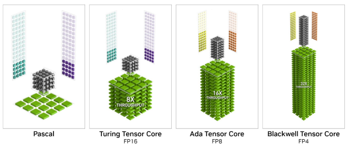
5th Generation Tensor Cores: Accelerating AI Inference
| 6000 Blackwell Max-Q | H100 PCIe | |
|---|---|---|
| Tensor Cores / SM | 4 (5th Gen) | 4 (4th Gen) |
One of the major features of the Blackwell generation is the 5th generation Tensor Core. FP4 and FP6, which were not supported by the 4th generation Tensor Cores, are now newly supported at the hardware level. Additionally, the Transformer Engine has been updated to its second generation.
Changes Across the Entire Chip
Next, let’s compare the GPUs at the full-chip level instead of focusing on a single SM.
| 6000 Blackwell Max-Q | H100 PCIe | |
|---|---|---|
| NVIDIA CUDA Cores | 24,064 | 14,592 |
| GPCs | 12 | 7 or 8 |
| TPCs | 94 | 57 |
| SMs | 188 | 114 |
| SMs / GPCs | 15.7 | 16.3 |
| RT Cores | 188 (4th Gen) | N/A |
| L1 Cache / SM (KB) | 128 | 256 |
| L2 Cache (MB) | 128 | 50 |
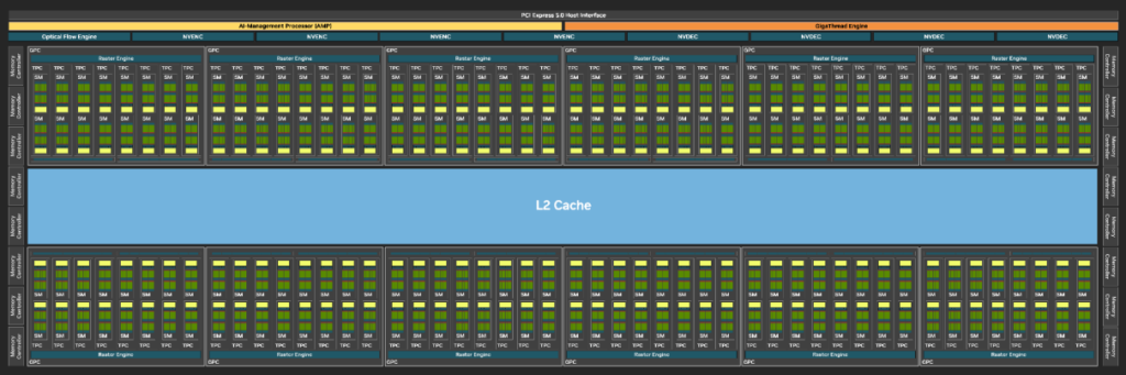
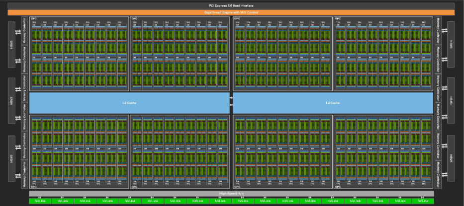
These diagrams show the full-size versions (GB202, GH100) of the chips used in the 6000 Blackwell Max-Q and H100 PCIe, respectively. The actual chips in each GPU may differ from these full-size versions, with some SMs disabled due to semiconductor manufacturing yields.
First, looking at the 6000 Blackwell Max-Q’s chip, the L2 cache, which was split into two partitions in the H100 PCIe, is now unified into a single block. Furthermore, the L2 cache size has been increased from 50 MB in the H100 PCIe to 128 MB in the 6000 Blackwell Max-Q. This increase makes it easier for data to fit within the L2 cache, which should be advantageous for workloads that use a lot of memory.
Also, the number of SMs is greater in the 6000 Blackwell Max-Q compared to the H100 PCIe. Specifically, the H100 PCIe has 114 SMs, while the 6000 Blackwell Max-Q has 188. A higher number of SMs can be advantageous for scheduling thread blocks in workloads with many fine-grained tasks.
A higher number of SMs also means more arithmetic units. The difference in FP32 performance between the two GPUs is thought to be due to this difference in SM count.
Large 96GB GDDR7 Memory
| 6000 Blackwell Max-Q | H100 PCIe | |
|---|---|---|
| GPU Memory | 96 GB GDDR7 | 80 GB HBM2e |
| Memory Interface (bit) | 512 | 5120 |
| Memory Data Rate (Gbps) | 28 | 3.19 |
| Memory Bandwidth (GB/sec) | 1792 | 2039 |
| PCIe Standard | Gen 5 | Gen 5 |
One of the major changes with the evolution to the Blackwell architecture is the memory.
In terms of memory capacity, a key feature of the 6000 Blackwell Max-Q is its 96 GB, even for a workstation GPU. This surpasses the 80 GB of the H100 PCIe. It will be highly effective for memory-intensive tasks and those handling large-scale machine learning models.
The 6000 Blackwell Max-Q adopts the new “GDDR7” memory standard. Compared to its predecessor, the RTX 6000 Ada (960 GB/sec), which also used GDDR, the memory bandwidth has increased significantly to 1792 GB/sec. The H100 PCIe, on the other hand, uses a standard called HBM2e. HBM2e achieves high bandwidth through a very wide bus but is more complex and expensive to manufacture than GDDR. It’s noteworthy that the 6000 Blackwell Max-Q achieves a vast bandwidth of 1792 GB/sec, which is close to the H100 PCIe’s 2039 GB/sec.
Based on these points, the 6000 Blackwell Max-Q is a suitable hardware choice for processes that utilize large amounts of memory.
Power Efficiency
| 6000 Blackwell Max-Q | H100 PCIe | |
|---|---|---|
| Power Consumption | 300 W | 350 W |
A key feature of the 6000 Blackwell Max-Q is its excellent power efficiency for a workstation. Its power consumption is 300 W, which is lower than the H100 PCIe’s 350 W.
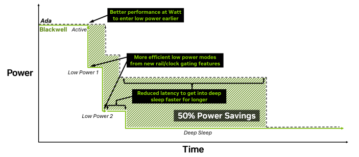
Furthermore, as its name suggests, it uses Max-Q technology. A feature of Max-Q technology is its ability to adjust power consumption at finer time intervals and for smaller units on the chip, allowing for a quicker transition to low-power states. New clock gating allows for clock speed adjustments at finer granularities and time scales. Power management for memory has also been improved, utilizing the fast startup and clock architecture of the GDDR7 memory adopted in Blackwell. New voltage lines have also been added, enabling voltage adjustments at a more granular level across the chip. For these reasons, the 6000 Blackwell Max-Q is considered to have its power efficiency optimized for on-demand workloads.
Conclusion
In this article, I have summarized the performance of the 6000 Blackwell Max-Q based on its datasheet. In future articles, I will test it hands-on to verify its performance, so please look forward to it.
Performance Comparison Table
| 6000 Blackwell Max-Q | H100 PCIe | RTX 5090 | RTX 6000 Ada | |
|---|---|---|---|---|
| Architecture | Blackwell (GB202) | Hopper (GH100) | Blackwell (GB202) | Ada Lovelace (AD102) |
| FP64 Performance (TFLOPS) | 1.71 | 25.6 | 1.64 | 1.42 |
| FP32 Performance (TFLOPS) | 109.7 | 51.2 | 104.8 | 91.1 |
| INT32 Performance (TOPS) | 109.7 | 25.6 | 104.8 | 44.5 |
| TF32 Performance (TFLOPS) | 438.9 | 756 | 209.5 | 364.2 |
| INT8 Performance (TOPS) | 1755.7 | 3026 | 1676 | 1457 |
| FP8 Perf (FP16 Accum) (TFLOPS) | 1755.7 | 3026 | 838 | 1457 |
| FP8 Perf (FP32 Accum) (TFLOPS) | 1755.7 | 3026 | 838 | 1457 |
| FP4 Perf (FP32 Accum) (TFLOPS) | 3511.4 | N/A | 3352 | N/A |
| RT Core Performance (TFLOPS) | 332.6 | N/A | 317.5 | 210.6 |
| NVIDIA CUDA Cores | 24,064 | 14,592 | 21,760 | 18,176 |
| GPCs | 12 | 7 or 8 | 11 | 12 |
| TPCs | 94 | 57 | 85 | 71 |
| SMs | 188 | 114 | 170 | 142 |
| RT Cores | 188 (4th Gen) | N/A | 170 (4th Gen) | 142 (3rd Gen) |
| CUDA Cores / SM | 128 | 128 | 128 | 128 |
| FP32 Cores / SM | 128 | 128 | 128 | 128 |
| FP64 Cores / SM | 2 | 64 | 2 | 2 |
| INT32 Cores / SM | 128 | 64 | 128 | 64 |
| Tensor Cores / SM | 4 (5th Gen) | 4 (4th Gen) | 4 (5th Gen) | 4 (4th Gen) |
| GPU Memory | 96 GB GDDR7 | 80 GB HBM2e | 32 GB GDDR7 | 48 GB GDDR6 |
| Memory Interface (bit) | 512 | 5120 | 512 | 384 |
| Memory Data Rate (Gbps) | 28 | 3.19 | 28 | 20 |
| Memory Bandwidth (GB/sec) | 1792 | 2039 | 1792 | 960 |
| L1 Cache / SM (KB) | 128 | 256 | 128 | 128 |
| L2 Cache (MB) | 128 | 50 | 96 | 96 |
| PCIe Standard | Gen 5 | Gen 5 | Gen 5 | Gen 4 |
| Power Consumption (W) | 300 | 350 | 575 | 300 |
References
AKIBA PC Hotline! Editorial Dept. 2023a. “The ‘NVIDIA RTX PRO 6000 Blackwell Max-Q Workstation Edition’ Featuring 96GB VRAM Launches for Approx. 1.6 Million Yen.” 2023. https://akiba-pc.watch.impress.co.jp/docs/news/news/2034324.html.
———. 2023b. “Oliospec Starts Accepting Orders for the ‘NVIDIA H100 Tensor Core GPU,’ Priced at Approx. 4.71 Million Yen.” 2023. https://akiba-pc.watch.impress.co.jp/docs/news/news/1500186.html.
NVIDIA. 2023a. “NVIDIA RTX BLACKWELL GPU ARCHITECTURE.” 2023. https://images.nvidia.com/aem-dam/Solutions/geforce/blackwell/nvidia-rtx-blackwell-gpu-architecture.pdf.
———. 2023b. “NVIDIA H100 Tensor Core GPU Architecture.” 2023. https://resources.nvidia.com/en-us-hopper-architecture/nvidia-h100-tensor-c.
———. 2023c. “NVIDIA ADA LOVELACE PROFESSIONAL GPU ARCHITECTURE.” https://images.nvidia.com/aem-dam/en-zz/Solutions/technologies/NVIDIA-ADA-GPU-PROVIZ-Architecture-Whitepaper_1.1.pdf.
———. 2025a. “CUDA C++ Best Practices Guide.” 2025. https://docs.nvidia.com/cuda/cuda-c-best-practices-guide/index.html#throughput-of-native-arithmetic-instructions.
———. 2025b. “NVIDIA Forum – Blackwell Integer.” 2025. https://forums.developer.nvidia.com/t/blackwell-integer/320578/137.
———. 2025c. “NVIDIA RTX PRO BLACKWELL GPU ARCHITECTURE.” 2025. https://www.nvidia.com/content/dam/en-zz/Solutions/design-visualization/quadro-product-literature/NVIDIA-RTX-Blackwell-PRO-GPU-Architecture-v1.0.pdf.